Texas Instruments LMS3655-Q1 Handleiding
Texas Instruments Niet gecategoriseerd LMS3655-Q1
Bekijk gratis de handleiding van Texas Instruments LMS3655-Q1 (61 pagina’s), behorend tot de categorie Niet gecategoriseerd. Deze gids werd als nuttig beoordeeld door 10 mensen en kreeg gemiddeld 4.1 sterren uit 6 reviews. Heb je een vraag over Texas Instruments LMS3655-Q1 of wil je andere gebruikers van dit product iets vragen? Stel een vraag
Pagina 1/61
LMS3635-Q1 3.5-A, LMS3655-Q1 5.5-A, 36-V Synchronous, 400-kHz Step-Down
Converter
1 Features
•AEC-Q100-qualified for automotive applications
–Device temperature grade 1: –40°C to +125°C
ambient operating temperature
–Device HBM classification level 2
–Device CDM classification level C6
•96% Peak efficiency while converting 12 V to 5 V
•Low EMI and minimized switch node ringing
•400-kHz (±10%) fixed switching frequency
•–40°C to +150°C junction temperature range
•External frequency synchronization
•RESET output with internal filter and 3-ms release
timer
•Automatic light load mode for improved efficiency
•Pin-selectable forced PWM mode
•Built-In compensation, soft start, current limit,
thermal shutdown, and UVLO
•0.35-V dropout with 3.5-A Load at 25°C (Typical)
•18-µA I
Q_VIN
: quiescent current at 3.3 V
OUT
and no
load (typical)
•Output voltage: 5 V, 3.3 V, and ADJ (1 V to 20 V)
•±1.5% reference voltage tolerance
•Create a custom design using the LMS3655-Q1
with the WEBENCH
®
Power Designer
2 Applications
•Automotive USB charge
•Driver monitoring
•Surround view system ECU
•Mechanically scanning LIDAR
•Vehicle to vehicle
3 Description
The LMS3635-Q1 and LMS3655-Q1 synchronous
buck regulators are optimized for high performance
applications, providing an output voltage of 3.3 V, 5
V, or an adjustable output of 1 V to 20 V. Seamless
transition between PWM and PFM modes, along with
a low quiescent current, ensures high efficiency and
superior transient responses at all loads.
Advanced high-speed circuitry allows the LMS3655-
Q1 to regulate an input of 24 V to an output of 3.3 V
at a fixed frequency of 400 kHz while also enabling
a continuous load current of 5.5 A. An innovative
frequency foldback architecture allows this device to
regulate a 3.3-V output from an input voltage of only
3.5 V. The input voltage can range up to 36 V, with
transient tolerance up to 42 V, easing input surge
protection design.
An open-drain reset output, with built-in filtering and
delay, provides a true indication of system status.
This feature negates the requirement for an additional
supervisory component, saving cost and board space.
Device Information
DEVICE NAMEPACKAGE
(1)
BODY SIZE
LMS3635-Q1
SON (22)4.00 mm × 5.00 mm
LMS3655-Q1
(1)For all available packages, see the orderable addendum at
the end of the data sheet.
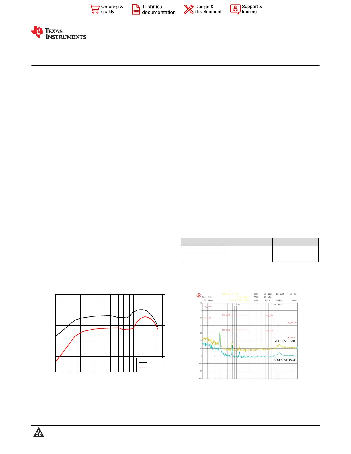
Output Current (A)
Efficiency
0.0010.010.1110
80%
82%
84%
86%
88%
90%
92%
94%
96%
98%
100%
LMS3
V
IN
= 12
V
IN
= 24
LMS3655-Q1 Efficiency: V
OUT
= 5 V
LMS3655-Q1 Conducted EMI: V
OUT = 5 V
, I
OUT
= 5 A
LMS3655-Q1, LMS3635-Q1
SNAS714C – NOVEMBER 2016 – REVISED AUGUST 2021
An IMPORTANT NOTICE at the end of this data sheet addresses availability, warranty, changes, use in safety-critical applications,
intellectual property matters and other important disclaimers. PRODUCTION DATA.
Product specificaties
| Merk: | Texas Instruments |
| Categorie: | Niet gecategoriseerd |
| Model: | LMS3655-Q1 |
Heb je hulp nodig?
Als je hulp nodig hebt met Texas Instruments LMS3655-Q1 stel dan hieronder een vraag en andere gebruikers zullen je antwoorden
Handleiding Niet gecategoriseerd Texas Instruments

9 Juni 2026
9 Juni 2026
9 Juni 2026
9 Juni 2026
8 Juni 2026
8 Juni 2026
6 Juni 2026
4 Juni 2026
3 Juni 2026
2 Juni 2026
Handleiding Niet gecategoriseerd
Nieuwste handleidingen voor Niet gecategoriseerd
9 Juni 2026
9 Juni 2026
9 Juni 2026
9 Juni 2026
9 Juni 2026
9 Juni 2026
9 Juni 2026
9 Juni 2026
9 Juni 2026