Texas Instruments LMK5C33216 Handleiding
Texas Instruments Niet gecategoriseerd LMK5C33216
Bekijk gratis de handleiding van Texas Instruments LMK5C33216 (94 pagina’s), behorend tot de categorie Niet gecategoriseerd. Deze gids werd als nuttig beoordeeld door 4 mensen en kreeg gemiddeld 4.8 sterren uit 5 reviews. Heb je een vraag over Texas Instruments LMK5C33216 of wil je andere gebruikers van dit product iets vragen? Stel een vraag
Pagina 1/94
LMK5C33216 Ultra-Low Jitter Clock Synchronizer with JESD204B for Wireless
Communications with BAW
1 Features
•BAW APLL with 40 fs RMS jitter at 491.52 MHz
•Three high-performance digital phase locked loops
(DPLLs) with paired analog phase locked loops
(APLLs)
–Programmable DPLL loop bandwidth from 0.01
Hz to 4 kHz
–-116 dBc/Hz at 100 Hz offset at 122.88 MHz
DPLL TDC noise with ≥ 20 MHz TDC rate
•Two differential or single-ended DPLL inputs
–1 Hz to 800 MHz differential
–Hitless switching with phase cancellation and/or
phase slew control
–Priority based reference selection
•16 outputs with programmable format
–1000 MHz LVPECL/LVDS/HSDS
–3000 MHz CML on OUT4 and OUT6
–200 MHz LVCMOS on OUT0 and OUT1
•Single 3.3-V supply with internal LDOs
•I
2
C or 3-wire/4-wire SPI interface
•Requires single XO/TCXO/OCXO
•40-bit DPLL or APLL DCO, < 1 ppt
•Holdover with phase build out upon exit
•Zero delay mode with programmable delay
•User programmable EEPROM
•Supports 105 °C PCB temperature
2 Applications
•4G and 5G Wireless Networks
•Base Band Unit (BBU)
•Active Antenna Unit (AAU)
•Remote Radio Unit (RRU)
•Network Switch (5G HUB)
•Small Cell
3 Description
The LMK5C33216 is a high-performance network
clock generator, synchronizer, and jitter attenuator
with advanced reference clock selection and
hitless switching capabilities designed to meet
the stringent requirements of communications
infrastructure applications.
The LMK5C33216 integrates 3 DPLLs with
programmable loop bandwidth and no external loop
filters, maximizing flexibility and ease of use. Each
DPLL phase locks a paired APLL to a DPLL reference
input. The APLL reference determines the long term
frequency accuracy.
The 3 APLLs may operate independent of their paired
DPLL and be cascaded from another APLL to provide
programmable frequency translation. APLL3 features
ultra high performance PLL with TI's proprietary
Bulk Acoustic Wave (BAW) VCBO technology and
can generate output clocks with 40-fs RMS jitter
independent of the jitter and frequency of the XO and
reference inputs. APLL1 and APLL2 provide options
for additional frequency domains.
The device is fully programmable through I
2
C or SPI
interface. The onboard EEPROM can be used to
customize system start-up clocks.
Device Information
(1)
PART
NUMBER
INOUTPACKAGE
BODY SIZE
(NOM)
LMK5C33216216VQFN (64)
9.00 mm ×
9.00 mm
(1)For all available packages, see the orderable addendum at
the end of the data sheet.
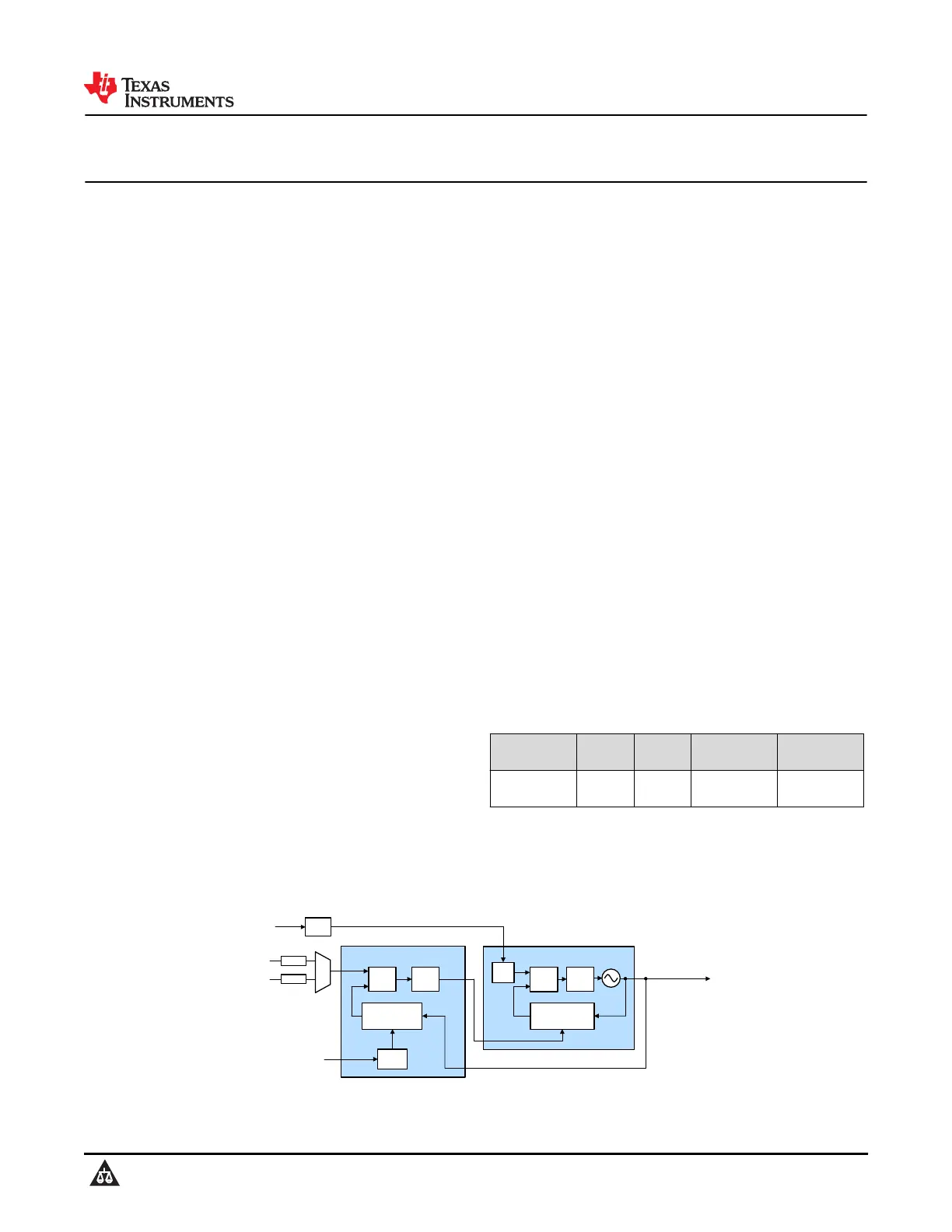
APLL
PFD
XO
f
PD
f
VCO
DPLL
TDCLF
÷R
16-bit
IN
0
:
IN
N
DCO option
DCO
FDEV
DPLL feedback clock
38-bit
÷FB
40-bit Frac-N SDM
÷N
40-bit Frac-N SDM
f
TDC
DLF
To post-divider
and
Output Muxes
FINC/FDEC
÷R
5-bit
×1, ×2
VCO
÷R
:
Figure 3-1. Block Diagram of Paired DPLL and APLL
www.ti.com
LMK5C33216
SNAS750B – NOVEMBER 2020 – REVISED MARCH 2021
Copyright ©2021 Texas Instruments Incorporated
Submit Document Feedback
1
Product Folder Links: LMK5C33216
LMK5C33216
SNAS750B – NOVEMBER 2020 – REVISED MARCH 2021
An IMPORTANT NOTICE at the end of this data sheet addresses availability, warranty, changes, use in safety-critical applications,
intellectual property matters and other important disclaimers. PRODUCTION DATA.
Product specificaties
| Merk: | Texas Instruments |
| Categorie: | Niet gecategoriseerd |
| Model: | LMK5C33216 |
Heb je hulp nodig?
Als je hulp nodig hebt met Texas Instruments LMK5C33216 stel dan hieronder een vraag en andere gebruikers zullen je antwoorden
Handleiding Niet gecategoriseerd Texas Instruments

9 Juni 2026
9 Juni 2026
9 Juni 2026
9 Juni 2026
8 Juni 2026
8 Juni 2026
6 Juni 2026
4 Juni 2026
3 Juni 2026
2 Juni 2026
Handleiding Niet gecategoriseerd
Nieuwste handleidingen voor Niet gecategoriseerd
9 Juni 2026
9 Juni 2026
9 Juni 2026
9 Juni 2026
9 Juni 2026
9 Juni 2026
9 Juni 2026
9 Juni 2026
9 Juni 2026
9 Juni 2026