Texas Instruments CDCDB400 Handleiding
Texas Instruments Niet gecategoriseerd CDCDB400
Bekijk gratis de handleiding van Texas Instruments CDCDB400 (33 pagina’s), behorend tot de categorie Niet gecategoriseerd. Deze gids werd als nuttig beoordeeld door 2 mensen en kreeg gemiddeld 5.0 sterren uit 7 reviews. Heb je een vraag over Texas Instruments CDCDB400 of wil je andere gebruikers van dit product iets vragen? Stel een vraag
Pagina 1/33
CDCDB400 DB800ZL-Compliant 4-Output Clock Buffer for PCIe Gen 1 to Gen 7
1 Features
•4 LP-HCSL outputs with programmable integrated
85Ω (default) or 100Ω differential output
terminations
•4 hardware output enable (OE#) controls
•Additive phase jitter after PCIE Gen 7 filter: 11.3fs,
RMS (maximum)
•Additive phase jitter after PCIE Gen 6 filter: 16.1fs,
RMS (maximum)
•Additive phase jitter after PCIE Gen 5 filter: 25fs,
RMS (maximum)
•Additive phase jitter after DB2000Q filter: 38fs,
RMS (maximum)
•Supports Common Clock (CC) and Individual
Reference (IR) architectures
–Spread spectrum-compatible
•Output-to-output skew: < 50ps
•Input-to-output delay: < 3ns
•Fail-safe input
•Programmable output slew rate control
•3 selectable SMBus addresses
•3.3V core and IO supply voltages
•Hardware-controlled low power mode (PD#)
•Current consumption: 46mA maximum
•5mm × 5mm, 32-pin VQFN package
2 Applications
•Microserver & tower server
•Storage area network & host bus adapter card
•Network attached storage
•Hardware accelerator
•Rack server
•Communications switch
•Computer on module
•CT & PET scanners
•Rugged PC laptop
3 Description
The CDCDB400 is a 4-output LP-HCSL, DB800ZL-
compliant, clock buffer capable of distributing the
reference clock for PCIe Gen 1-7, QuickPath
Interconnect (QPI), UPI, SAS, and SATA interfaces
in CC, SRNS, or SRIS architectures. The SMBus
interface and four output enable pins allow the
configuration and control of all four outputs
individually. The CDCDB400 is a DB800ZL derivative
buffer and meets or exceeds the system parameters
in the DB800ZL specification. The device also
meets or exceeds the parameters in the DB2000Q
specification. The CDCDB400 is packaged in a 5mm
× 5mm, 32-pin VQFN package.
Package Information
PART NUMBERPACKAGE
(1)
PACKAGE SIZE
(2)
CDCDB400VQFN (32)5.00mm × 5.00mm
(1)For all available packages, see the orderable addendum at
the end of the data sheet.
(2)The package size (length × width) is a nominal value and
includes pins, where applicable.
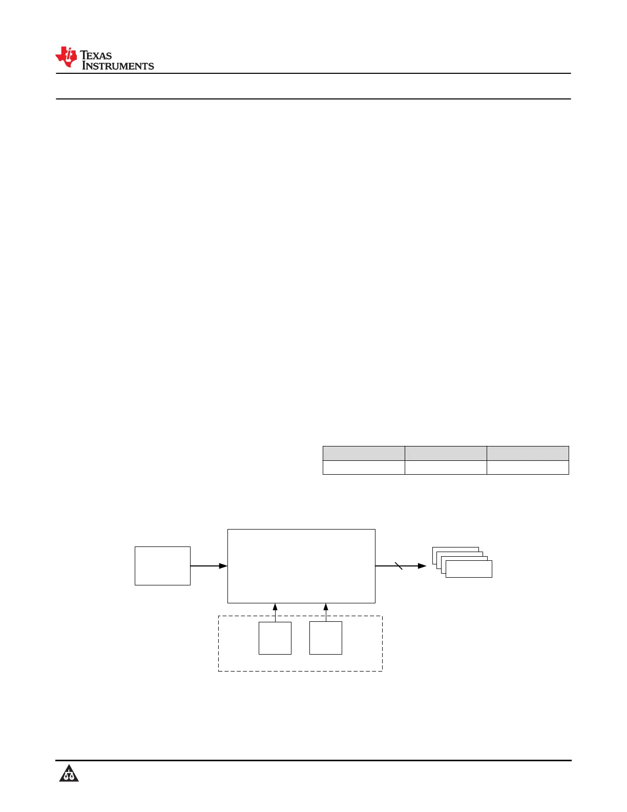
PCIe Gen 4-5
Clock
Generator
CDCDB400
4x LP-HSCL Output Buffer
SMBus
Control
OE#
Control
LP-HCSL
PCIe PHY
LP-HCSL
4
PCIe PHY
PCIe PHY
PCIe Device
Control Interface
CDCDB400 System Diagram
CDCDB400
SNAS833B – NOVEMBER 2021 – REVISED AUGUST 2025
An IMPORTANT NOTICE at the end of this data sheet addresses availability, warranty, changes, use in safety-critical applications,
intellectual property matters and other important disclaimers. PRODUCTION DATA.
Product specificaties
| Merk: | Texas Instruments |
| Categorie: | Niet gecategoriseerd |
| Model: | CDCDB400 |
Heb je hulp nodig?
Als je hulp nodig hebt met Texas Instruments CDCDB400 stel dan hieronder een vraag en andere gebruikers zullen je antwoorden
Handleiding Niet gecategoriseerd Texas Instruments

23 April 2026
22 April 2026
21 April 2026
21 April 2026
20 April 2026
14 April 2026
14 April 2026
13 April 2026
13 April 2026
11 April 2026
Handleiding Niet gecategoriseerd
Nieuwste handleidingen voor Niet gecategoriseerd
25 April 2026
25 April 2026
25 April 2026
25 April 2026
25 April 2026
25 April 2026
25 April 2026
25 April 2026
25 April 2026
24 April 2026