Microchip MIC45404 Handleiding


Lees hieronder de 📖 handleiding in het Nederlandse voor Microchip MIC45404 (34 pagina's) in de categorie Niet gecategoriseerd. Deze handleiding was nuttig voor 97 personen en werd door 2 gebruikers gemiddeld met 4.5 sterren beoordeeld

Pagina 1/34
2015-2017 Microchip Technology Inc. DS20005478B-page 1
MIC45404
Features
Input Voltage Range: 4.5V to 19V
Output Current: Up to 5A
82% Peak Efficiency at 12 VIN, 0.9 VOUT
Pin-Selectable Output Voltages: 0.7V, 0.8V, 0.9V,
1.0V, 1.2V, 1.5V, 1.8V, 2.5V, 3.3V
±1% Output Voltage Accuracy
Supports Safe Pre-Biased Start-Up
Pin-Selectable Current Limit
Pin-Selectable Switching Frequency
Internal Soft Start
Thermal Shutdown
Hiccup Mode Short-Circuit Protection
Available in a 54-Lead 6 mm x 10 mm QFN
Package
Ultra-Low Profile: 2.0 mm Height
-40°C to +125°C Junction Temperature Range
Applications
Servers, Data Storage, Routers and Base Stations
FPGAs, SSD, DSP and Low-Voltage ASIC Power
General Description
The MIC45404 device is an ultra-low profile, synchro-
nous step-down regulator module, featuring a unique
2.0 mm height. The module incorporates a DC-to-DC
regulator, bootstrap capacitor, high-frequency input
capacitor and an inductor in a single package. The
module pinout is optimized to simplify the Printed
Circuit Board (PCB) layout process.
This highly-integrated solution expedites system
design and improves product time to market. The inter-
nal MOSFETs and inductor are optimized to achieve
high efficiency at low output voltage. Due to the fully
optimized design, MIC45404 can deliver up to 5A
current with a wide input voltage range of 4.5V to 19V.
The MIC45404 is available in a 54-lead 6 mm x
10 mm x 2.0 mm QFN package with a junction operat-
ing temperature range from -40C to +125C, which
makes an excellent solution for systems in which PCB
real-estate and height are important limiting factors,
and air flow is restricted.
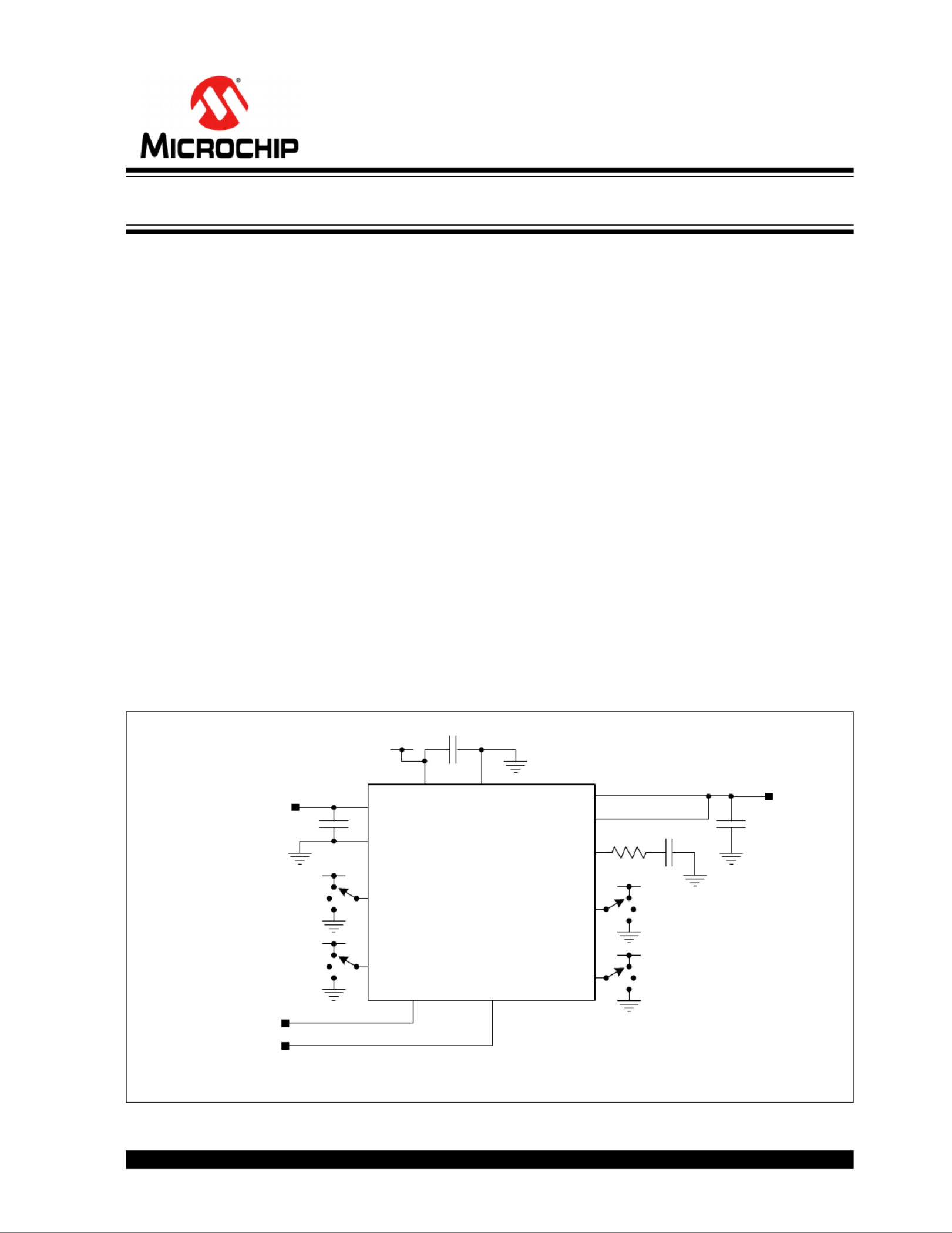
Typical Application
VIN
OUT
VIN
4.5V to 19V
FREQ
VDDA
VOSET1
PG
GND
GND
VOSET0
COMP
EN/DLY
OUTSNS
MIC45404
V
DDA
Power-Good
Enable
VDDA
VDDA
Output
Voltage
Selection
VDDA
Frequency
Selection
ILIM
VDDA
Current Limit
Selection
VOUT
MIC45404 12V 5A DC-to-DC Converter
19V 5A Ultra-Low Profile DC-to-DC Power Module
MIC45404
DS20005478B-page 2 2015-2017 Microchip Technology Inc.
Package Types
Functional Diagram
MIC45404
6 mm x 10 mm QFN*
(Top View)
8
26
22
24
23
3
37
35
34
25
47
46
7
KEEPOUT
GND
GND
BST
PG
VDDA
LX
OUT
GND
21
KEEPOUT
48
38
4
1
2
AGND
VOSET1
NC
41
43
53
OUTSNS
EN/DLY
33
VOSET0
LX
44
45
VDDP
31
30
29
32
52
36
28
20
9
LX
LX
LX
LX
LX
LX
LX
LX
LX
OUT
OUT
12
OUT13
OUT14
OUT15
OUT16
OUT17
OUT18
OUT19
GND
VIN
VIN
27
LX
LX
39
40
LX
KEEPOUT
BST 42
NC
ILIM
49
FREQ
50
51
GND
COMP
54
OUTSNS
KEEPOUT10
OUT11
6 GND_EXT
5 GND_EXT
MIC45404YMP
GND_EP
* Includes Exposed Thermal Pad (EP); see Table 3-1.
LX
BST
ILIM
FREQ
VDDA
VOSET1
PG
AGND
VOSET0
COMP
EN/DLY
OUTSNS
VIN
PGND
VDDP
PWM
Regulator
100 nF
47 pF
LX
BST
VOSET1
AGND
VOSET0
GND_EP
OUTSNS
GND
COMP
OUT
ILIM
FREQ
VDDA
PG
EN/DLY
VIN
VDDP
GND_EXT
VDDP
LDO
VIN
2015-2017 Microchip Technology Inc. DS20005478B-page 3
MIC45404
1.0 ELECTRICAL CHARACTERISTICS
Absolute Maximum Ratings†
VIN to AGND ................................................................................................................................................ -0.3V to +20V
VDDP
, VDDA to AGND ..................................................................................................................................... -0.3V to +6V
VDDP to VDDA ............................................................................................................................................ -0.3V to +0.3V
VOSETX, FREQ, ILIM, to AGND .................................................................................................................... -0.3V to +6V
BST to LX..................................................................................................................................................... -0.3V to +6V
BST to AGND .............................................................................................................................................. -0.3V to +26V
EN/DLY to AGND...................................................................................................................... -0.3V to V
DDA + 0.3V, +6V
PG to AGND .................................................................................................................................................. -0.3V to +6V
COMP, OUTSNS to A
GND ....................................................................................................... -0.3V to V
DDA + 0.3V, +6V
AGND to GND ............................................................................................................................................ -0.3V to +0.3V
Junction Temperature .......................................................................................................................................... +150°C
Storage Temperature (TS)...................................................................................................................... -65°C to +150°C
Lead Temperature (soldering, 10s) ........................................................................................................................ 260°C
ESD Rating
( )1
HBM ........................................................................................................................................................................... 2kV
MM ........................................................................................................................................................................... 150V
CDM....................................................................................................................................................................... 1500V
Note 1: Devices are ESD-sensitive. Handling precautions are recommended. Human body model, 1.5 k in series
with 100 pF.
Operating Ratings( )1
Supply Voltage (VIN) ..................................................................................................................................... 4.5V to 19V
Externally Applied Analog and Drivers Supply Voltage (V
IN = VDDA = VDDP).............................................. 4.5V to 5.5V
Enable Voltage (EN/DLY)............................................................................................................................... 0V to V
DDA
Power Good (PG) Pull-up Voltage (VPU_PG) ................................................................................................ 0V to 5.5V
Output Current ............................................................................................................................................................. 5A
Junction Temperature (TJ) ..................................................................................................................... -40°C to +125°C
Note 1: The device is not ensured to function outside the operating range.
† Notice: Stresses above those listed under “Maximum Ratings” may cause permanent damage to the device. This is
a stress rating only and functional operation of the device at those or any other conditions above those indicated in
the operational sections of this specification is not intended. Exposure to maximum rating conditions for extended
periods may affect device reliability.


Product specificaties

Merk: Microchip
Categorie: Niet gecategoriseerd
Model: MIC45404

Heb je hulp nodig?

Als je hulp nodig hebt met Microchip MIC45404 stel dan hieronder een vraag en andere gebruikers zullen je antwoorden


Handleiding Niet gecategoriseerd Microchip

Handleiding Niet gecategoriseerd

Nieuwste handleidingen voor Niet gecategoriseerd