Microchip TC1321 Handleiding


Lees hieronder de 📖 handleiding in het Nederlandse voor Microchip TC1321 (39 pagina's) in de categorie Niet gecategoriseerd. Deze handleiding was nuttig voor 19 personen en werd door 2 gebruikers gemiddeld met 4.5 sterren beoordeeld

Pagina 1/39
 2000 Microchip Technology Inc. Preliminary DS00735A-page 1
INTRODUCTION
This application note describes the implementation of
the PICmicro MSSP module for Master I2C communi-
cations. The Master Synchronous Serial Port (MSSP)
module is the enhanced Synchronous Serial Port
developed by Microchip Technology and is featured on
many of the PICmicro devices. This module provides
for both the 4-mode SPI communications, as well as
Master and Slave I2C communications, in hardware.
For information on the SPITM peripheral implementation
see the PICmicroTM Mid-Range MCU Family Reference
Manual, document DS33023. The MSSP module in I
2C
mode fully implements all Master and Slave functions
(including general call support) and provides interrupts
on START and STOP bits in hardware to determine a
free I2C bus (multi-master function). The MSSP module
implements the standard mode specifications, as well
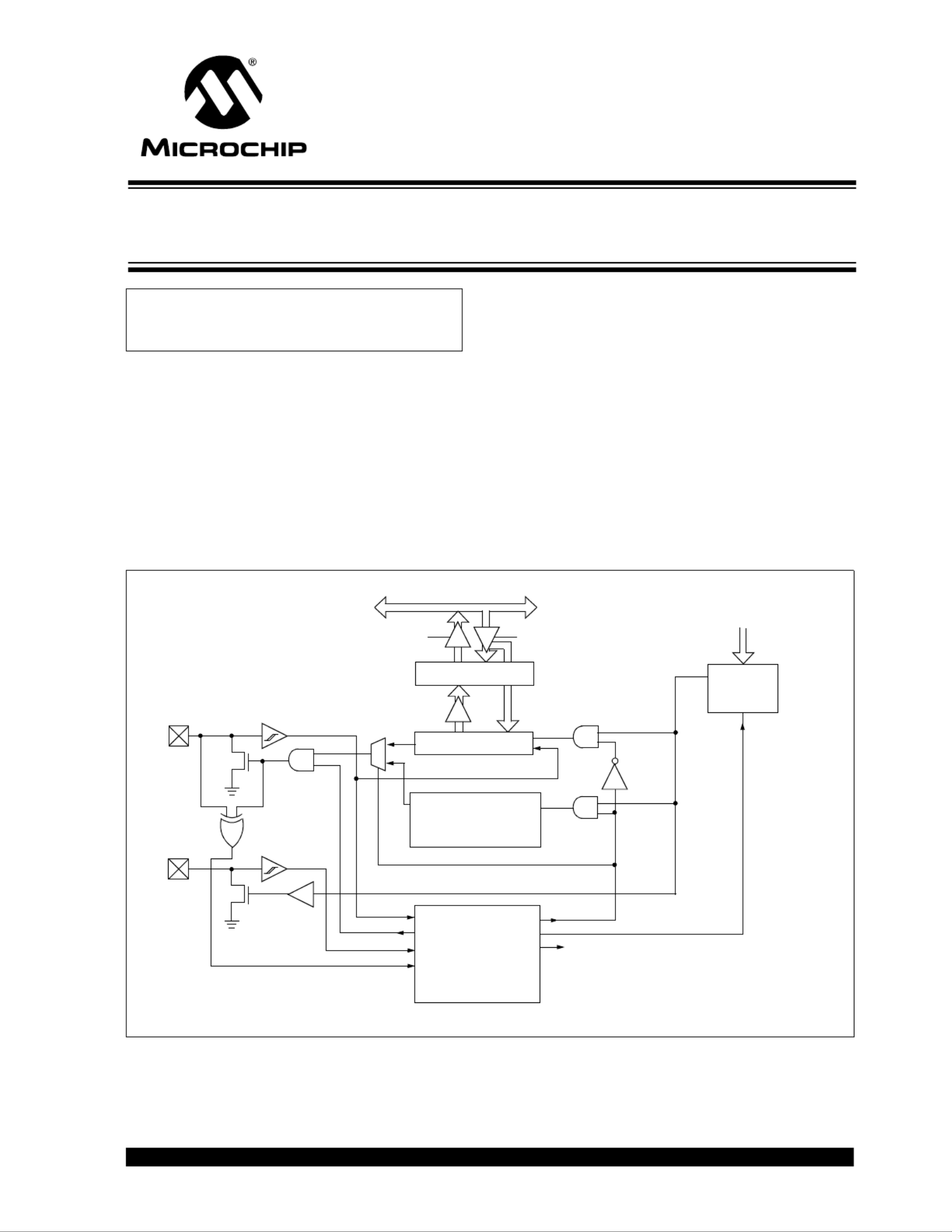
as 7-bit and 10-bit addressing. Figure 1 depicts a func-
tional block diagram of the I2C Master mode. The appli-
cation code for this I2C example is developed for and
tested on a PIC16F873, but can be ported over to a
PIC17CXXX and PIC18CXXX PICmicro MCU which
features a MSSP module.
FIGURE 1: I2C MASTER MODE BLOCK DIAGRAM
Author: Richard L. Fischer
Microchip Technology Inc.
Read Write
SSPSR
START bit, STOP bit,
SSPBUF
Internal
Data Bus
Set/Reset, S, P, WCOL (SSPSTAT)
Shift
Clock
MSb LSb
SDA
Acknowledge
Generate
SCL
SCL In
Bus Collision
SDA In
Receive Enable
Clock cntl
Clock Arbitrate/WCOL Detect
(hold off clock source)
SSPADD<6:0>
Baud
Set SSPIF, BCLIF
Reset ACKSTAT, PEN (SSPCON2)
Rate
Generator
SSPM3:SSPM0
START bit detect
STOP bit detect
Write collision detect
Clock Arbitration
State counter for
end of XMIT/RCV
AN735
Using the PICmicro® MSSP Module for Master
I2CTM Communications
AN735
DS00735A-page 2 Preliminary  2000 Microchip Technology Inc.
THE I2C BUS SPECIFICATION
Although a complete discussion of the I
2C bus specifi-
cation is outside the scope of this application note,
some of the basics will be covered here. For more infor-
mation on the I2C bus specification, you may refer to
sources indicated in the References section.
The Inter-Integrated-Circuit, or I2C bus specification
was originally developed by Philips Inc. for the transfer
of data between ICs at the PCB level. The physical
interface for the bus consists of two open-collector
lines; one for the clock (SCL) and one for data (SDA).
The SDA and SCL lines are pulled high by resistors
connected to the VDD rail. The bus may have a one
Master/many Slave configuration or may have multiple
master devices. The master device is responsible for
generating the clock source for the linked Slave
devices.
The I2C protocol supports either a 7-bit addressing
mode, or a 10-bit addressing mode, permitting 128 or
1024 physical devices to be on the bus, respectively. In
practice, the bus specification reserves certain
addresses so slightly fewer usable addresses are avail-
able. For example, the 7-bit addressing mode allows
112 usable addresses. The 7-bit address protocol is
used in this application note.
All data transfers on the bus are initiated by the master
device and are done eight bits at a time, MSb first.
There is no limit to the amount of data that can be sent
in one transfer. After each 8-bit transfer, a 9th clock
pulse is sent by the master. At this time, the transmit-
ting device on the bus releases the SDA line and the
receiving device on the bus acknowledges the data
sent by the transmitting device. An ACK (SDA held low)
is sent if the data was received successfully, or a NACK
(SDA left high) is sent if it was not received success-
fully. A NACK is also used to terminate a data transfer
after the last byte is received.
According to the I2C specification, all changes on the
SDA line must occur while the SCL line is low. This
restriction allows two unique conditions to be detected
on the bus; a START sequence (S) and a STOP
sequence (P). A START sequence occurs when the
master device pulls the SDA line low while the SCL line
is high. The START sequence tells all Slave devices on
the bus that address bytes are about to be sent. The
STOP sequence occurs when the SDA line goes high
while the SCL line is high, and it terminates the trans-
mission. Slave devices on the bus should reset their
receive logic after the STOP sequence has been
detected.
The I2C protocol also permits a Repeated Start condi-
tion (Rs), which allows the master device to execute a
START sequence without preceding it with a STOP
sequence. The Repeated Start is useful, for example,
when the Master device changes from a write operation
to a read operation and does not release control of the
bus.
MSSP MODULE SETUP,
IMPLEMENTATION AND CONTROL
The following sections describe the setup, implemen-
tation and control of the PICmicro MSSP module for
I2C Master mode. Some key Special Function Regis-
ters (SFRs) utilized by the MSSP module are:
1. SSP Control Register1 (SSPCON1)
2. SSP Control Register2 (SSPCON2)
3. SSP Status Register (SSPSTAT)
4. Pin Direction Control Register (TRISC)
5. Serial Receive/Transmit Buffer (SSPBUF)
6. SSP Shift Register (SSPSR) - Not directly
accessible
7. SSP Address Register (SSPADD)
8. SSP Hardware Event Status (PIR1)
9. SSP Interrupt Enable (PIE1)
10. SSP Bus Collision Status (PIR2)
11. SSP Bus Collision Interrupt Enable (PIE2)
Module Setup
To configure the MSSP module for Master I2C mode,
there are key SFR registers which must be initialized.
Respective code examples are shown for each.
1. SSP Control Register1 (SSPCON1)
• I2C Mode Configuration
2. SSP Address Register (SSPADD<6:0>)
• I2C Bit Rate
3. SSP Status Register (SSPSTAT)
• Slew Rate Control
• Input Pin Threshold Levels (SMbus or I2C)
4. Pin Direction Control (TRISC)
• SCL/SDA Direction
To configure the MSSP module for Master I2C mode,
the SSPCON1 register is modified as shown in
Example 1.
EXAMPLE 1: I2C MODE CONFIGURATION
With the two-wire synchronous I2C bus, the Master
generates all clock signals at a desired bit rate. Using
the formula in Equation 1, the bit rate can be calculated
and written to the SSPADD register. For a 400kHz bit
rate @ Fosc = 16MHz, the SSPADD register is modi-
fied as shown in Example 2.
movlw b’00101000’ ; setup value
; into W register
banksel SSPCON1 ; select SFR
; bank
movwf SSPCON1 ; configure for
; Master I 2C
AN735
 2000 Microchip Technology Inc. Preliminary DS00735A-page 3
EQUATION 1: BIT RATE CALCULATION
EXAMPLE 2: I2C BIT RATE SETUP
To enable the slew rate control for a bit rate of 400kHz
and select I2C input thresholds, the SSPSTAT register
is modified as shown in Example 3.
EXAMPLE 3: SLEW RATE CONTROL
The SSPSTAT register also provides for read-only
status bits which can be utilized to determine the status
of a data transfer, typically for the Slave data transfer
mode. These status bits are:
•D/A - Data/Address
•P - STOP
•S - START
•R/W - Read/Write Information
•UA - Update Address (10-bit mode only)
•BF - Buffer Full
Finally, before selecting any I2C mode, the SCL and
SDA pins must be configured to inputs by setting the
appropriate TRIS bits. Selecting an I2C mode by set-
ting the SSPEN bit (SSPCON1<5>), enables the SCL
and SDA pins to be used as the clock and data lines in
I2C mode. A logic "1" written to the respective TRIS bits
configure these pins as inputs. An example setup for a
PIC16F873 is shown in Example 4. Always refer to the
respective data sheet for the correct SCL and SDA
TRIS bit locations.
EXAMPLE 4: SCL/SDA PIN DIRECTION
SETUP
The four remaining SFR’s can be used to provide for
I2C event completion and Bus Collision interrupt func-
tionality.
1. SSP Event Interrupt Enable bit (SSPIE)
2. SSP Event Status bit (SSPIF)
3. SSP Bus Collision Interrupt Enable bit (BCLIE)
4. SSP Bus Collision Event Status bit (BCLIF)
Implementation and Control
Once the basic functionality of the MSSP module is
configured for Master I2C mode, the remaining steps
relate to the implementation and control of I
2C events.
The Master can initiate any of the following I
2C bus
events:
1. START
2. Restart
3. STOP
4. Read (Receive)
5. Acknowledge (after a read)
•Acknowledge
•Not Acknowledge (NACK)
6. Write
The first four events are initiated by asserting high the
appropriate control bit in the SSPCON2<3:0> register.
The Acknowledge bit event consists of first setting the
Acknowledge state, ACKDT (SSPCON2<5>) and then
asserting high the event control bit ACKEN
(SSPCON2<4>).
Data transfer with acknowledge is obligatory. The
acknowledge related clock is generated by the Master.
The transmitter releases the SDA line (HIGH) during
the acknowledge clock pulse. The receiver must pull
down the SDA line during the acknowledge clock pulse
so that it remains stable LOW during the HIGH period
of this clock pulse. This sequence is termed "ACK" or
acknowledge.
When the Slave doesn’t acknowledge the Master dur-
ing this acknowledge clock pulse (for any reason), the
data line must be left HIGH by the Slave. This
sequence is termed "NACK" or not acknowledge.
Example 5 shows an instruction sequence which will
generate an acknowledge event by the Master.
EXAMPLE 5: ACKNOWLEDGE EVENT
movlw b’00001001’ ; setup value
; into W register
banksel SSPADD ; select SFR bank
movwf SSPADD ; baud rate =
; 400KHz @ 16MHz
movlw b’00000000’ ; setup value
; into W register
movwf SSPSTAT ; slew rate
; enabled
banksel SSPSTAT ; select SFR bank
movlw b’00011000’ ; setup value
; into W register
banksel TRISC ; select SFR bank
iorwf TRISC,f ; SCL and SDA
; are inputs
SSPADD =
FOSC
Bit Rate
4
- 1
(
)
banksel SSPCON2 ; select SFR
; bank
bcf SSPCON2, ACKDT ; set ack bit
; state to 0
bsf SSPCON2, ACKEN ; initiate ack


Product specificaties

Merk: Microchip
Categorie: Niet gecategoriseerd
Model: TC1321

Heb je hulp nodig?

Als je hulp nodig hebt met Microchip TC1321 stel dan hieronder een vraag en andere gebruikers zullen je antwoorden


Handleiding Niet gecategoriseerd Microchip

Handleiding Niet gecategoriseerd

Nieuwste handleidingen voor Niet gecategoriseerd