Microchip MCP2515 Handleiding
Microchip Niet gecategoriseerd MCP2515
Bekijk gratis de handleiding van Microchip MCP2515 (96 pagina’s), behorend tot de categorie Niet gecategoriseerd. Deze gids werd als nuttig beoordeeld door 15 mensen en kreeg gemiddeld 4.7 sterren uit 2 reviews. Heb je een vraag over Microchip MCP2515 of wil je andere gebruikers van dit product iets vragen? Stel een vraag
Pagina 1/96
2003-2021 Microchip Technology Inc.DS20001801K-page 1
MCP2515
Features
•Implements CAN V2.0B at 1 Mb/s:
-0 to 8-byte length in the data field
-Standard and extended data and remote
frames
•Receive Buffers, Masks and Filters:
-Two receive buffers with prioritized message
storage
-Six 29-bit filters
-Two 29-bit masks
•Data Byte Filtering on the First Two Data Bytes
(applies to standard data frames)
•Three Transmit Buffers with Prioritization and
Abort Features
•High-Speed SPI Interface (10MHz):
-SPI Modes 0,0 and 1,1
•One-Shot mode Ensures Message Transmission
is Attempted Only One Time
•Clock Out Pin with Programmable Prescaler:
-Can be used as a clock source for other
device(s)
•Start-of-Frame (SOF) Signal is Available for
Monitoring the SOF Signal:
-Can be used for time slot-based protocols
and/or bus diagnostics to detect early bus
degradation
•Interrupt Output Pin with Selectable Enables
•Buffer Full Output Pins Configurable as:
-Interrupt output for each receive buffer
-General purpose output
•Request-to-Send (RTS) Input Pins Individually
Configurable as:
-Control pins to request transmission for each
transmit buffer
-General purpose inputs
•Low-Power CMOS Technology:
-Operates from 2.7V-5.5V
-5 mA active current (typical)
-1 µA standby current (typical) (Sleep mode)
•Temperature Ranges Supported:
-Industrial (I): -40°C to +85°C
-Extended (E): -40°C to +125°C
•AEC-Q100 Qualified
Description
Microchip Technology’s MCP2515 is a stand-alone
Controller Area Network (CAN) controller that imple-
ments the CAN specification, Version 2.0B. It is capable
of transmitting and receiving both standard and
extended data and remote frames. The MCP2515 has
two acceptance masks and six acceptance filters that
are used to filter out unwanted messages, thereby
reducing the host MCU’s overhead. The MCP2515
interfaces with microcontrollers (MCUs) via an industry
standard Serial Peripheral Interface (SPI).
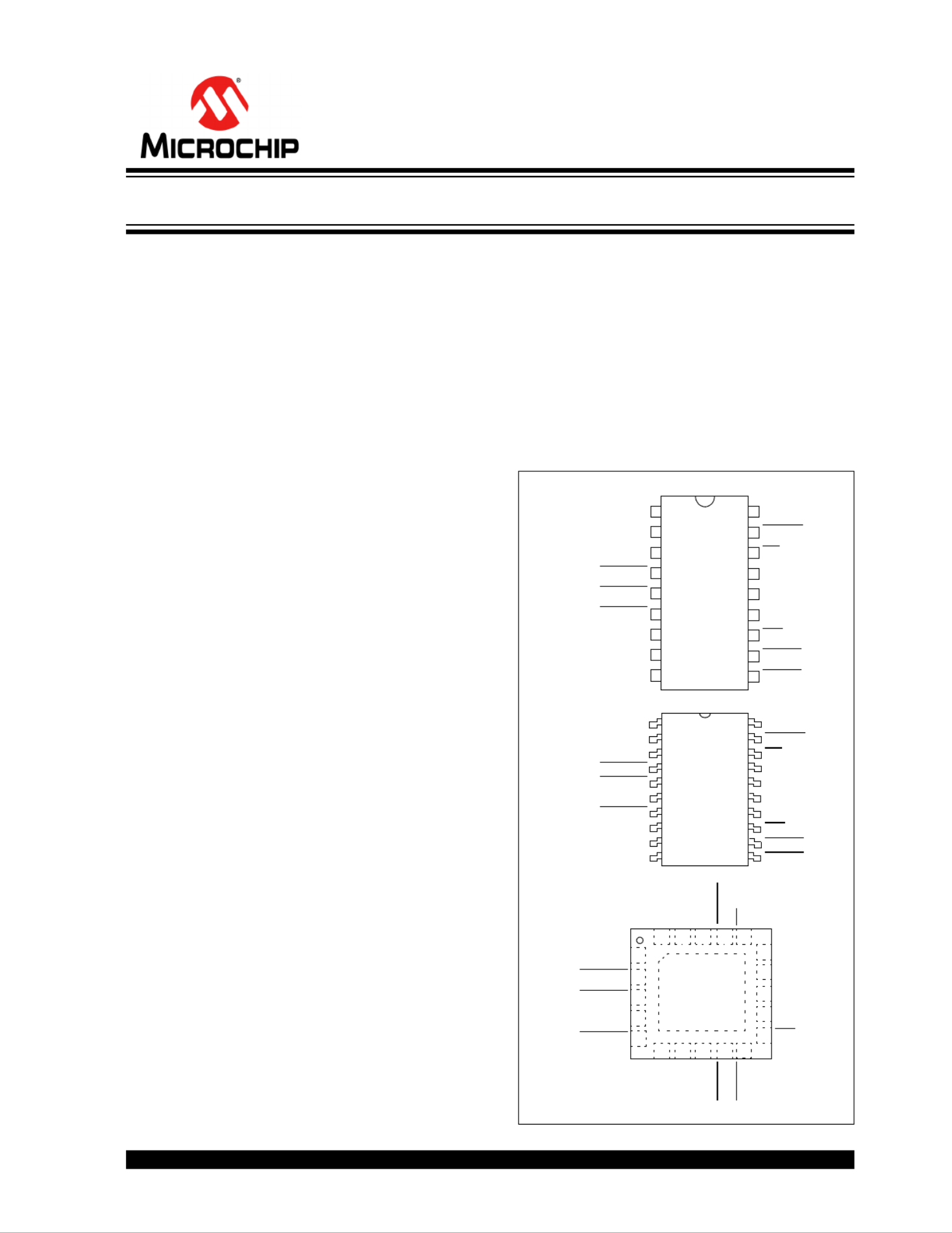
Package Types
16
5
TXCAN
RXCAN
VDD
RESET
CS
SO
MCP2515
1
2
3
4
18
17
16
15
SI
SCK
INT
RX0BF
14
13
12
11
RX1BF10
OSC2
OSC1
CLKOUT/SOF
TX2RTS
5
6
7
8
VSS 9
TX0RTS
TX1RTS
TXCAN
RXCAN
TX0RTS
OSC1
CLKOUT/SOF
OSC2
CS
VDD
RESET
SO
SCK
INT
SI
RX0BF
RX1BF
VSS
TX1RTS
TX2RTS
NC NC
18-Lead PDIP/SOIC
20-Lead TSSOP
2
NC
TX2RTS
TX0RTS
SO
SI
OSC2
NC
OSC1
GND
RX1BF
SCK
RXCAN
TXCAN
VDD
RESET
TX1RTS
EP
20
1
19 18 17
3
4
14
13
12
11
6 7 89
21
10
15
CLKOUT
CS
INT
RX0BF
* Includes Exposed Thermal Pad (EP); see Table 1-1.
13
12
1
2
3
4
5
6
7
8
9
20
19
18
17
16
15
14
11
10
MCP2515
20-Lead QFN*
Stand-Alone CAN Controller with SPI Interface
Product specificaties
| Merk: | Microchip |
| Categorie: | Niet gecategoriseerd |
| Model: | MCP2515 |
Heb je hulp nodig?
Als je hulp nodig hebt met Microchip MCP2515 stel dan hieronder een vraag en andere gebruikers zullen je antwoorden
Handleiding Niet gecategoriseerd Microchip

2 Februari 2026
26 Januari 2026
13 Januari 2026
12 Januari 2026
12 Januari 2026
12 Januari 2026
12 Januari 2026
12 Januari 2026
6 December 2025
5 December 2025
Handleiding Niet gecategoriseerd
Nieuwste handleidingen voor Niet gecategoriseerd
12 Juni 2026
12 Juni 2026
12 Juni 2026
12 Juni 2026
12 Juni 2026
11 Juni 2026
11 Juni 2026
11 Juni 2026
11 Juni 2026
11 Juni 2026