Microchip HV738DB1 Handleiding


Lees hieronder de 📖 handleiding in het Nederlandse voor Microchip HV738DB1 (10 pagina's) in de categorie Niet gecategoriseerd. Deze handleiding was nuttig voor 19 personen en werd door 2 gebruikers gemiddeld met 4.5 sterren beoordeeld

Pagina 1/10
Supertex inc.
Supertex inc.
www.supertex.com
HV738DB1
Doc.# DSDB-HV738DB1
B070114
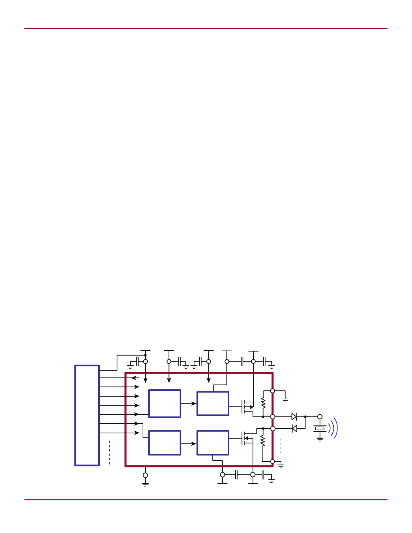
Designing a Pulser with HV738
This demoboard data sheet describes how to use the
HV738DB1 to generate the basic high voltage pulse
waveform as an ultrasound transmitting pulser.
The HV738 circuit uses the DC coupling method in all
level translators. There are no external coupling capacitors
needed. The VPP and VNN rail voltages can be changed
rather quickly, compared to a high voltage capacitor gate
coupled driving pulser. This direct coupling topology of the
gate drivers not only saves two high voltage capacitors per
channel, but also makes the PCB layout easier.
The input stage of the HV738 has high-speed level
translators that are able to operate with logic signals of 1.2
to 5.0V and are optimized at 2.5 to 3.3V. In this demoboard,
the control logic signals are connected to a high-speed
ribbon cable connector. The control signal logic-high voltage
should be the same as the VCC voltage of the demoboard,
and the logic-low should be reference to GND.
The HV738DB1 output waveforms can be displayed by using
an oscilloscope probe directly connected to the test point
TX1~4 and GND. The soldering jumper can select whether
or not to connect the on-board equivalent-load, a 330pF,
200V capacitor, parallel with a 2.5kΩ, 1W resistor. Also, a
coaxial cable can be used to connect the user’s transducer
to easily drive and evaluate the HV738 transmitter pulser.
Typical Application Circuit
HV738 ±65V 0.75A
Ultrasound Pulser Demoboard
Introduction
The HV738 is a monolithic four channel, high speed, high
voltage, ultrasound transmitter pulser. This integrated, high
performance circuit is in a single 7x7mm, 48-lead QFN
package.
The HV738 can deliver up to ±0.75A source and sink
current to a capacitive transducer. It is designed for
medical ultrasound imaging and ultrasound material NDT
applications. It can also be used as a high voltage driver
for other piezoelectric or capacitive MEMS transducers, or
for ATE systems and pulse signal generators as a signal
source.
HV738’s circuitry consists of controller logic circuits, level
translators, gate driving buffers and a high current and
high voltage MOSFET output stage. The output stages of
each channel are designed to provide peak output currents
over ±1.1A for pulsing, when MC0 = 1 and MC1 = 1, with
up to ±65V swings. When in mode 1, all the output stages
drop the peak current to ±140mA for low-voltage CW mode
operation to save power. Two oating 8.0VDC power
supplies, referenced to VPP and VNN, supply the P- and N-type
power FET gate drivers. This pulser waveform’s frequency
upper limit is 20MHz depending on the load capacitance.
One HV738 can also be used as four damping circuits to
generate fast return-to-zero waveforms by working with
another HV738 as four pulsing circuits. It also has built-in
under-voltage and over-temperature protection functions.
Level
Translator
V
PP
-8V
V
PF
V
DD
+8.0V
V
PP
V
NN
0 to -65V
TXN1
V
NN
+ 8V
N-Driver
1 of 4 Channels Shown
TXP1 HV
OUT
1
V
NF
V
SUB
V
LL
+2.5V +65V
V
SS
VCC
OTP
EN
MC0
MC1
PIN1
NIN1
GREF
GND
GND
Logic
Control
0V to +65V
RGND
P-Driver
HV738
Level
Translator
RGND
2
HV738DB1
Supertex inc.
www.supertex.com
Doc.# DSDB-HV738DB1
B070114
The PCB Layout Techniques
The large thermal pad at the bottom of the HV738 package
is connected to the VSUB pins to ensure that it always has
the highest potential of the chip, in any condition. VSUB is
the connection of the IC’s substrate. PCB designers need to
pay attention to the connecting traces as the output TXP1~4,
TXN1~4 high-voltage and high-speed traces. In particular,
low capacitance to the ground plane and more trace spacing
need to be applied in this situation.
High-speed PCB trace design practices that are compatible
with about 50 to 100MHz operating speeds are used for the
demoboard PCB layout. The internal circuitry of the HV738
can operate at quite a high frequency, with the primary speed
limitation being load capacitance. Because of this high speed
and the high transient currents that result when driving
capacitive loads, the supply voltage bypass capacitors and
the driver to the FET’s gate-coupling capacitors should be
as close to the pins as possible. The VSS pin pads should
have low inductance feed-through connections that are
connected directly to a solid ground plane. The VDD, VPP, VPF,
VNF and VNN supplies can draw fast transient currents of up
to ±1.5A, so they should be provided with a low-impedance
bypass capacitor at the chip’s pins. A ceramic capacitor of
up to 0.22 to 1.0µF may be used. Minimize the trace length
to the ground plane, and insert a ferrite bead in the power
supply lead to the capacitor to prevent resonance in the
power supply lines. For applications that are sensitive to
jitter and noise and using multiple HV738 ICs, insert another
ferrite bead between VDD and decouple each chip supply
separately.
Pay particular attention to minimizing trace lengths and
using sufîš¿cient trace width to reduce inductance. Surface
mount components are highly recommended. Since the
output impedance of HV738’s high voltage power stages are
very low, in some cases it may be desirable to add a small
value resistor in series with the output TXP1~4 and TXN1~4
to obtain better waveform integrity at the load terminals.
This will, of course, reduce the output voltage slew rate at
the terminals of a capacitive load. Be aware of the parasitic
coupling from the outputs to the input signal terminals of
HV738. This feedback may cause oscillations or spurious
waveform shapes on the edges of signal transitions. Since
the input operates with signals down to 1.2V, even small
coupling voltages may cause problems. Use of a solid
ground plane and good power and signal layout practices
will prevent this problem. Also ensure that the circulating
ground return current from a capacitive load cannot react
with common inductance to create noise voltages in the
input logic circuitry.
Testing the Integrated Pulser
This HV738 pulser demoboard should be powered up with
multiple lab DC power supplies with current limiting functions.
The following power supply voltages and current limits have
been used in the testing: VPP = 0 to +65V 5.0mA, VNN = 0 to
-65V 5.0mA, VDD = +8.0V 10mA, (VPP - VPF) = +8.0V 10mA,
(VNF - VNN) = +8.0V 10mA. VCC = +2.5V 5.0mA for HV738 VLL
does not include the user’s logic circuits.
The power-up or down sequences of the voltage supply
ensure that the HV738 chip substrate VSUB is always at the
highest potential of all the voltages supplied to the IC.
The (VPP - VPF) and (VNF - VNN) are the two oating power
supplies. They are only 8.0V, but oating with VPP and VNN.
The oating voltages can be trimmed within the range of
+7.5 to +10V to match the rising and falling time of the output
pulses for the best HD2. Do not exceed the maximum voltage
of +10V. The VPP and VNN are the positive and negative high
voltages. They can be varied from 0 to +/-65V maximum.
Note when the VPP = VNN =0, the VPF and VNF in respect to the
ground voltage is -8.0V and +8.0V.
The on-board dummy load 330pF//2.5kΩ should be
connected to the high voltage pulser output through the
solder jumper when using an oscilloscope’s high impedance
probe to meet the typical loading conditions. To evaluate
different loading conditions, one may change the values of
RC within the current and power limit of the device.
In order to drive piezo transducers with a cable, one should
match the output load impendence properly to avoid cable
and transducer reections. A 70 to 75Ω coaxial cable is
recommended. The coaxial cable end should be soldered
to the TX1~4 and GND directly with very short leads. If a
user’s load is being used, the on board dummy load should
be disconnected by cutting the small shorting copper trace
in between the zero ohm resistors R7, R8, R9 or R10 pads.
They are shorted by factory default.
All the on-board test points are designed to work with the
high impedance probe of the oscilloscope. Some probes
may have limited input voltage. When using the probe
on these high voltage test-points, make sure that VPP/VNN
voltages do not exceed the probe limit. Using the high
impendence oscilloscope probe for the on-board test points,
it is important to have short ground leads to the circuit board
ground plane.
Precautions need to be applied to not overlap the logic-high
time periods of the control signals. Otherwise, permanent
damage to the device may occur when cross-conduction or
shoot-through current exceed the device’s maximum limits.
3
HV738DB1
Supertex inc.
www.supertex.com
Doc.# DSDB-HV738DB1
B070114
Schematic
Board Layout
TP16
3
1
2
VDD
TP1
VSUB
TX3
NIN3
R15
10
TP7
TP23
3
1
2
V
SUB
VCC
TX4
C3
0.22
TP9
R16
10
C7
0.22
PIN3
TP6
1
2
3
4
5
6
7
8
VNN
R17
10
C4
0.22
TP10
43
D8B
NIN4
VDD
PIN1
R4
10
PIN4
TP15
VPP
VPP
NIN1
TP11
OTP
3
1
2
D1
BAV99
TP12
1 6
D8A
BAT54DW-7
2 1
D5
B1100-13
TP25
C6
0.22
TP13
MC1
TX1
TP2
TP17
VCC
V
PP
TP5 C5
1µ
100V
1
2
3
4
5
6
7
8
9
10
11
12
13
14
15
16
17
18
19
2021
22
23
24
25
26
27
28
29
30
31
32
33
34
35
3637
38
39
40
41
42
43
44
45
46
47
48
TP18
VCC
R11
1K
V
PF
2 1
D7
B1100-13
VCC
TP19
TP4
V
PF
TP20
C2
0.22
MC0
V
NN
R12
1
VSUB
VCC
R5
0
NIN2
VSUB
V
DD
C12
0.22
4 3
D6B
V
NF
EN
1 6
D6A
BAT54DW-7
21
D9
B1100-13
VDD
VNN
C13
0.22
TP22
VNF
V
NN
R13
10
VNF
TP8
3
1
2
TX2
21
D10
B1100-13
VPF
PIN2
VPP
J1
HEADER
12X2
VPP
R14
10
VDD
VSS
PIN1
NIN1
PIN2
NIN2
PIN3
NIN3
PIN4
NIN4
VSS
VDD
OTP
MC1
MC0
VSUB
VPF
VPP
VPP
VPPVNN
VNN
VNN
VNF
VSUB
RGND
TXN4
TXP4
TXN3
TXP3
TXN2
TXP2
TXN1
TXP1
RGND
VSUBVNF
VNN
VNN
VNN
VPP
VPP
VPP
VPF
VSUB
EN
GREF
VLL
U1
HV738K6
C9
1µ
100V
C8
1µ
100V
C15
1µ
100V
C14
1µ
100V
J2 8HEADER
+65V > VSUB > VPP
VCC = +3.3V
VDD = V+8
(VPP - VPF) = V+8
(VNF - VNN
) = V+8
VPP = 0 to +65V
VNN = 0 to -65V
BAT54DW-7
BAT54DW-7
TP24
R6
2.55K
1W
R10
0
C16
330p
250V
TP21
R3
2.55K
1W
R9
0
C11
330p
250V
TP14
R2
2.55K
1W
R8
0
C10
330p
250V
TP3
R1
2.55K
1W
R7
0
C1
330p
250V
D2
BAV99
D3
BAV99
D4
BAV99
1
3
5
7
9
11
13
15
17
19
21
23
2
4
6
8
10
12
14
16
18
20
22
24


Product specificaties

Merk: Microchip
Categorie: Niet gecategoriseerd
Model: HV738DB1

Heb je hulp nodig?

Als je hulp nodig hebt met Microchip HV738DB1 stel dan hieronder een vraag en andere gebruikers zullen je antwoorden


Handleiding Niet gecategoriseerd Microchip

Handleiding Niet gecategoriseerd

Nieuwste handleidingen voor Niet gecategoriseerd