Texas Instruments LMR36503-Q1 Handleiding
Texas Instruments Niet gecategoriseerd LMR36503-Q1
Bekijk gratis de handleiding van Texas Instruments LMR36503-Q1 (54 pagina’s), behorend tot de categorie Niet gecategoriseerd. Deze gids werd als nuttig beoordeeld door 2 mensen en kreeg gemiddeld 4.6 sterren uit 9 reviews. Heb je een vraag over Texas Instruments LMR36503-Q1 of wil je andere gebruikers van dit product iets vragen? Stel een vraag
Pagina 1/54
LMR36503-Q1 3-V to 65-V, 0.3-A Synchronous Buck Converter Optimized for Size and
Light Load Efficiency
1 Features
•AEC-Q100-qualified for automotive applications:
–Device temperature grade 1: –40°C to +125°C,
T
A
•Functional Safety-Capable
–Documentation available to aid functional safety
system design
•>70% efficiency at 5 mA
–4 µA I
Q
(switching) at 24 V
IN
to 3.3 V
OUT
(fixed
output option)
•Miniature solution size and low component cost
–2-mm × 2-mm HotRod
™
package with wettable
flanks
–Internal compensation
•Designed for automotive applications:
–Junction temperature range –40°C to +150°C
–Pseudo-random spread spectrum compatible
with CISPR 25 EMI standard
–Wide input voltage range: 3.0 V (falling
threshold) to 65 V
–Adjustable, 3.3-V and 5-V fixed output voltage
options available
–Synchronizable with MODE/SYNC pin variant
–Adjustable F
SW
: 200 kHz to 2.2 MHz with RT
pin variant
–Pin compatible with LMR36506-Q1 (65 V, 600
mA)
2 Applications
•Advanced driver assistance systems (ADAS)
•Body electronics and lighting
•Infotainment and cluster
3 Description
The LMR36503-Q1 is the industry's smallest 65 V,
0.3 A synchronous step-down DC/DC converter in
2-mm x 2-mm HotRod
™
package. This easy-to-use
converter can handle input voltage transients up to
70 V, provide excellent EMI performance and support
fixed 3.3 V, 5 V and other adjustable output voltages.
The LMR36503-Q1 uses peak current mode control
architecture with internal compensation and maintains
stable operation with minimal output capacitance.
The wide input operating range of the LMR36503-
Q1 helps it remain functional during a deep input
voltage sag condition, making it an excellent choice
for automotive applications withstanding severe cold
crank start impulses. The PGOOD flag in the
LMR36503-Q1 provides precise indication of the
output voltage status, eliminating the requirement for
an external supervisor. A seamless transition from
FPWM to PFM, with an ultra-low standby quiescent
current allows the LMR36503-Q1 to support much
higher system efficiency at low output loads. The
MODE/SYNC pin variant helps to synchronize the
LMR36503-Q1 to an external clock. With the right
resistor selection, the LMR36503-Q1 RT pin variant
can also be externally programmed to any desired
switching frequency of operation. The rich feature
set of the LMR36503-Q1 is designed to simplify
implementation for a wide range of automotive end
equipments.
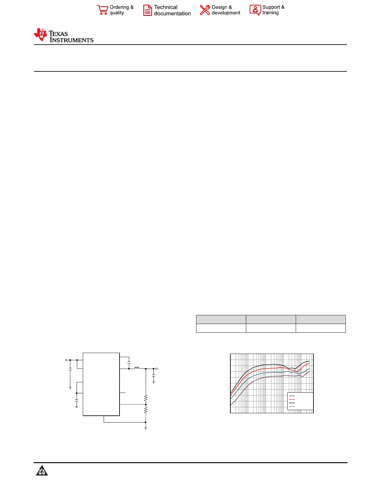
Device Information
PART NUMBERPACKAGE
(1)
BODY SIZE (NOM)
LMR36503-Q1VQFN-HR (9)2.00 mm × 2.00 mm
(1)For all available packages, see the orderable addendum at
the end of the data sheet.
V
IN
VIN
EN/
UVLO
BOOT
SW
FB
GND
V
OUT
C
BOOT
L
IND
C
IN
C
OUT
R
FBT
R
FBB
VCC
PGOOD
C
VCC
MODE/
SYNC
Simplified Schematic
Load Current (A)
Efficiency (%)
0
10
20
30
40
50
60
70
80
90
100
10P100P1m10m100m
LMR3
V
IN
= 8V
V
IN
= 13.5V
V
IN
= 24V
V
IN
= 48V
Efficiency versus Output Current V
OUT
= 3.3 V
(Fixed), 2.2 MHz
LMR36503-Q1
SNVSBB5B – SEPTEMBER 2019 – REVISED SEPTEMBER 2020
An IMPORTANT NOTICE at the end of this data sheet addresses availability, warranty, changes, use in safety-critical applications,
intellectual property matters and other important disclaimers. PRODUCTION DATA.
Product specificaties
| Merk: | Texas Instruments |
| Categorie: | Niet gecategoriseerd |
| Model: | LMR36503-Q1 |
Heb je hulp nodig?
Als je hulp nodig hebt met Texas Instruments LMR36503-Q1 stel dan hieronder een vraag en andere gebruikers zullen je antwoorden
Handleiding Niet gecategoriseerd Texas Instruments

9 Juni 2026
9 Juni 2026
9 Juni 2026
9 Juni 2026
8 Juni 2026
8 Juni 2026
6 Juni 2026
4 Juni 2026
3 Juni 2026
2 Juni 2026
Handleiding Niet gecategoriseerd
Nieuwste handleidingen voor Niet gecategoriseerd
9 Juni 2026
9 Juni 2026
9 Juni 2026
9 Juni 2026
9 Juni 2026
9 Juni 2026
9 Juni 2026
9 Juni 2026
9 Juni 2026