Microchip HV7350DB1 Handleiding


Lees hieronder de 📖 handleiding in het Nederlandse voor Microchip HV7350DB1 (10 pagina's) in de categorie Niet gecategoriseerd. Deze handleiding was nuttig voor 18 personen en werd door 2 gebruikers gemiddeld met 4.5 sterren beoordeeld

Pagina 1/10
Supertex inc.
Supertex inc.
www.supertex.com
HV7350DB1
Doc.# DSDB-HV7350DB1
A070214
General Description
The HV7350 is a monolithic eight channel, high-speed, high
voltage, ultrasound transmitter RTZ pulser. This integrated,
high performance circuit is in a single, 8x8x0.9 mm, 56-lead
QFN package.
The HV7350 can deliver a guaranteed ±1.0A source and
sink current to a capacitive transducer with +/-60V peak to
peak voltage. It is designed for portable medical ultrasound
imaging and ultrasound NDT applications. It can also be used
as a high voltage driver for other piezoelectric or capacitive
MEMS transducers, or for test systems as a signal source or
pulse signal generators.
The HV7350’s circuitry consists of controller logic circuits,
level translators, gate driving buffers and a high current and
high voltage MOSFET output stage. The output stages of
each channel are designed to provide peak output currents
typically over ±1.0A for pulsing, with up to ±60V swings in
RTZ mode. The upper limit frequency of the pulser waveform
is depending on the load capacitance.
This demoboard datasheet describes how to use the
HV7350DB1 to generate the basic high voltage pulse
waveform as an ultrasound transmitting pulser.
The HV7350 circuit uses DC coupling from a 3.3V logic
input to output Tx1~8 internally, therefore the chip needs
three sets of voltage supply rails: VLL +3.3V, VDD +5.0V and
VPP/VNN ±10 to ±60V. The VPP and VNN rail voltages can be
changed rather quickly, compared to the capacitor gate-
coupled driving pulsers. This direct coupling topology of the
gate drivers not only saves two high voltage capacitors per
channel, but also makes the PCB layout easier.
The HV7350DB1 output waveforms can be displayed using
an oscilloscope by connecting the scope probe directly to
the test points TX1~8 and GND. The soldering jumper can
select whether or not to connect the on-board dummy-load,
a 330pF capacitor paralleling with a 2.5kΩ resistor. The test
points can be used to connect the user’s transducer to easily
evaluate the pulser.
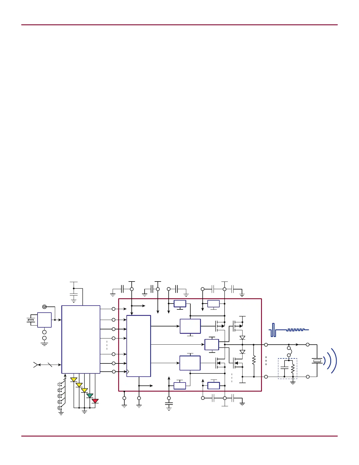
Block Diagram
Eight Channel ±60V, ±1.0A,
Ultrasound Pulser Demoboard
CPFVDD
+3.3V
RGND
HVOUT1
VPP
+10 to +60V
-10 to -60V
P-Driver
N-Driver
1 of 8 Channels
VLL
Logic
&
Level
Translator
-5V
RGND
RGND
DMP
1.0µF
VPF
VNF
Rb
LRP
+5.0V
CPOS
GND
GND
SUB
+4.0V
VREF
REN
OEN
PIN1
NIN1
PIN8
NIN8
CLK
DAP
LRP
GND
LRN
GND
VNF
VPF
LRN
GND
GND CNEG CNF VNN
+5.0V
-5.0V
1.0µF
1.0µF
0.1µF 1.0µF 1.0µF
TX1
+3.3V
1.0µ 1.0µF F
RGND
TX1
Waveform
Generator
CPLD
OSC
JTAG
EXCLK
EN
CLKIN
WAVE
FREQ
PHAS
OEN
REN
RTZ
PHAS
PWR
OEN
REN
40MHz
6
+3.3V
C4
330pF
R2
R3
2.5k
Dummy
Load
2
HV7350DB1
Supertex inc.
www.supertex.com
Doc.# DSDB-HV7350DB1
A070214
The PCB Layout Techniques
The large thermal pad at the bottom of the HV7350 package
is internally connected to the IC’s substrate (VSUB). This
thermal pad should be connected to 0V or GND externally on
the PCB. Designers need to pay attention to the connecting
traces on the outputs TX1~8, speciîš¿cally the high voltage and
high speed traces. In particular, controlled impedance to the
ground plane and more trace spacing needs to be applied in
this situation.
High speed PCB trace design practices that are compatible
with about 50 to 100MHz operating speeds are used for the
demoboard PCB layout. The internal circuitry of the HV7350
can operate at quite a high frequency, with the primary speed
limitation being load capacitance. Because of this high speed
and the high transient currents that result when driving ca-
pacitive loads, the supply voltage bypass capacitors and the
driver to the FET’s gate-coupling capacitors should be as
close to the pins as possible. The GND pin should have low
inductance feed-through via connections that are connected
directly to a solid ground plane. The VDD, VPP, VNN, CPF,
CNF, CNEG and CPOS voltage supply and/or bypass capaci-
tor pins can draw fast transient currents of up to 2.0A, so ±
they should be provided with a low impedance bypass capaci-
tor at the chip’s pins. A ceramic capacitor of 1.0 to 2.0µF may
be used. Only the VPP and VNN pins to GND capacitors need
to be the high-voltage type. The CPF to VPP and CNF to VNN
capacitors maybe low voltage. Minimize the trace length to
the ground plane, and insert a ferrite bead in the power supply
lead to the capacitor to prevent resonance in the power sup-
ply lines. For applications that are sensitive to jitter and noise
and using multiple HV7350 ICs, insert another ferrite bead
between each chip’s supply lines.
Pay particular attention to minimizing trace lengths and us-
ing sufîš¿cient trace width to reduce inductance. Surface mount
components are highly recommended. Since the output im-
pedance of the HV7350’s high voltage power stages is very
low, in some cases it may be desirable to add a small value
resistor in series with the output TX1~8 to obtain better wave-
form integrity at the load terminals after long cables. This will,
of course, reduce the output voltage slew rate at the terminals
of a capacitive load.
Be aware of the parasitic coupling from the outputs to the in-
put signal terminals of the HV7350. This feedback may cause
oscillations or spurious waveform shapes on the edges of the
signal transitions. Since the input operates with signals down
to 3.3V, even small coupling voltages may cause problems.
Use of a solid ground plane and good power and signal layout
practices will prevent this problem. Also ensure that the cir-
culating ground return current from a capacitive load cannot
react with common inductance to create noise voltages in the
input logic circuitry.
Testing the Integrated Pulser
The HV7350 pulser demoboard should be powered up with
multiple lab DC power supplies with current limiting functions.
The on-board dummy load 330pF//2.5k should be connectΩ-
ed to the high voltage pulser output through the solder jumper
when using an oscilloscope’s high impedance probe to meet
the typical loading condition. To evaluate different loading
conditions, one may change the values of RC within the cur-
rent and power limit of the device.
In order to drive the user’s piezo transducers with a cable, one
should match the output load impendence properly to avoid
cable and transducer reections. A 70 to 75Ω coaxial cable is
recommended. The coaxial cable end should be soldered to
the TX1~8 and GND directly with very short leads. If a user’s
load is being used, the on-board dummy load should be dis-
connected by cutting the small shorting copper trace in be-
tween the 0 resistors R2, R9, R12, R18, R23, R53, R54 or Ω
R55 pads. They are shorted by factory default.
All the on-board test points are designed to work with the
high impedance probe of the oscilloscope. Some probes may
have limited input voltage. When using the probe on these
high voltage test-points, make sure that VPP/VNN voltages do
not exceed the probe limit. Using the high impendence oscil-
loscope probe for the on-board test points, it is important to
have short ground leads to the circuit board ground plane.
If both of the inputs PIN and NIN are high, then the channel
out TX will be in Hi-Z.
3
HV7350DB1
Supertex inc.
www.supertex.com
Doc.# DSDB-HV7350DB1
A070214
HV7350DB1 Schematic
REN
OEN
PAD
VDD
VNN
VCC = +3.3V
VDD = +4.0 to 5.2V
VPP / VNN
= +/-5.0 to 70V
Note: J4-4, 5, 6 & 7- pins for test only
TP10
CLK
SYNC
EXTRG
U2
XC9572XL_VQ44
REN
OEN
PIN1
NIN1
PIN2
NIN2
PIN3
NIN3
PIN4
NIN4
PIN5
NIN5
PIN6
NIN6
PIN7
NIN7
PIN8
NIN8
TX1
TX2
TX3
TX4
TX5
TX6
TX7
TX8
RGND
RGND
RGND
RGND
RGND
RGND
VLL
VLL
VDD
VDD
CPF
CPF
VPP
VPP
VPP
VPP
VPP
VPP
17
54
19
52
48
23
20
21
22
49
50
51
MH3MH2 MH1MH4
D7
RED
D4
YLW
D6
GRN
R4
1.0k
D3
RED
D5
YLW
R5
1.0k
R6
1.0k
R7
1.0k
R8
1.0k
TP12
TP9
TP6
J2
EXCLK
EX=0
EN
1
GND
2OUT
VCC 4
40MHz X1
TP13
1
3
1
2
J1
C18
0.22
2
3
R14
1.0k 43
40
39
R15
50
VCC
TP30
EXTRG
TP18
R16
1k
R20
1k
C31
0.22
SW2
4
17
25
2
3
5
6
7
10
9
24
11
R25
33k
C32
0.22
C33
0.22
C34
0.22
C35
0.22
SW1 SW3 SW4 SW5
R26
33k
R27
33k
R28
33k
R29
33k
R40
200
R41
200
R42
200
R43
200
R44
200
VCC
C30
0.22
GND
GND
GND
WAV
FRE
SEL
ENA
MOD
TMS
TDI
TDO
TCK
SET
LE
MC
CS
EN
VCC
VCC
VCC
32
31
30
29
28
35
26
15
C1
022
C2
022
C3
022
VCC
U3
HV7350
C25
022 C19
022
TP2
C12
1µF C13
1µF
TP8
PIN1
NIN1
PIN2
NIN2
PIN3
NIN3
PIN4
NIN4
PIN5
NIN5
PIN6
NIN6
PIN7
NIN7
PIN8
NIN8
VCC
J3 JTAG
1
2
3
4
5
6
C22
0.22
RTZ
REN
PHAS
PWR
OEN
VCC VPP
C6
1µ
C9
1µ
C8
1µ
C5
1µ
TP35
TP6
8
7
55
56
1
2
3
4
5
6
9
10
11
12
13
14
15
16
38
37
34
33
22
21
20
19
18
16
14
13
12
8
42
41
TP50
TP51
TP49
TP48
TP47
TP46
TP45
TP44
TP29
TP28
TP27
TP25
TP22
TP19
TP20
TP16 43
41
39
37
34
32
30.
28
31
29
33
38
40
42
TX2
TX4
TX6
TX8
TX1
TX3
TX5
TX7
PAD
GND
GND
CPOS
CNEG
CNF
CNF
VNN
VNN
VNN
VNN
VNN
VNN
72
18
53
36
35
47
24
25
26
27
44
45
46
TP43
R52
2.55k
1W
C40
330P
250V
TP41
R55
0
R51
2.55k
1W
C39
330P
250V
TP39
R54
0
TP40
3
2
1
TP0
3
2
1
BAV99/SOT_1
D31
BAV99/SOT_1
D30
R56
2.55k
1W
C38
330P
250V
TP26
R53
0
R10
2.55k
1W
C14
330P
250V
TP7
R9
0
TP21
3
2
1
TP42
3
2
1
BAV99/SOT_1
D29
BAV99/SOT_1
D28
R24
2.55k
1W
C29
330P
250V
TP0
R23
0
R19
2.55k
1W
C21
330P
250V
TP31
R18
0
TP32
3
2
1
TP23
3
2
1
BAV99/SOT_1
D27
BAV99/SOT_1
D26
R13
2.55k
1W
C20
330P
250V
TP14
R12
0
R3
2.55
k
1W
C4
330P
250V
TP4
R2
0
TP11
3
2
1
TP1
3
2
1
BAV99/SOT_1
D25
BAV99/SOT_1
D24
C36
1µF
TP36
C37
1µF
TP17
C28
1µF
100v
C27
1µF
100v
TP33
C24
1µF
C23
1µF
6
141
1 2
2
3
VPPVDD VNNVCC
D20A
BAT54DW-7
D20B
BAT54DW-7
D17
B1100-13
D16
B1100-13
SYNC
CNEG CPOS
1
2
3
4
5
6
7
8
9
10
CNF CPF VPPVNNVDDVDD
J4 HEADER 10
R31
1
R30
1
R38
INF
R37
INF
R57
INF
R32
10
R35
10


Product specificaties

Merk: Microchip
Categorie: Niet gecategoriseerd
Model: HV7350DB1

Heb je hulp nodig?

Als je hulp nodig hebt met Microchip HV7350DB1 stel dan hieronder een vraag en andere gebruikers zullen je antwoorden


Handleiding Niet gecategoriseerd Microchip

Handleiding Niet gecategoriseerd

Nieuwste handleidingen voor Niet gecategoriseerd