Advantech PCI-1712 Handleiding
Advantech Niet gecategoriseerd PCI-1712
Bekijk gratis de handleiding van Advantech PCI-1712 (4 pagina’s), behorend tot de categorie Niet gecategoriseerd. Deze gids werd als nuttig beoordeeld door 18 mensen en kreeg gemiddeld 4.7 sterren uit 7 reviews. Heb je een vraag over Advantech PCI-1712 of wil je andere gebruikers van dit product iets vragen? Stel een vraag
Pagina 1/4
1 Startup Manual
STARTUP MANUAL
PCI-1712/1712L
1 MS/s, 12-bit, 16-ch High-Speed
Multifunction card
Before installation, please make sure that you have
received the following:
• PCI-1712, PCI-1712L card
• Driver CD
• Quick Start User Manual
If anything is missing or damaged, contact your
distributor or sales representative immediately.
For more detailed information on this product,
please refer to the PCI-1712 User Manual on the
CD-ROM (PDF format).
CD:\Documents\Hardware Manuals\PCI\PCI-1712
FCC Class A
This equipment has been tested and found to comply with
the limits for a Class A digital device, pursuant to part 15 of
the FCC Rules. These limits are designed to provide reason-
able protection against harmful interference when the
equipment is operated in a commercial environment. This
equipment generates, uses, and can radiate radio frequency
energy and, if not installed and used in accordance with the
instruction manual, may cause harmful interference to radio
communications. Operation of this equipment in a residen-
tial area is likely to cause interference in which case the
user is required to correct interference at his own expense.
CE
This product has passed the CE test for environmental spec-
ifications when shielded cables are used for external wiring.
We recommend the use of shielded cables. This kind of
cable is available from Advantech. Please contact your local
supplier for ordering information.
The PCI-1712/1712L is a powerful high-speed mul-
tifunction DAS card for PCI bus. It features a 1MHz
12-bit A/D converter, an on-board FIFO buffer
(storing up to 1K samples for A/D, and up to 32K
samples for D/A conversion). The PCI-1712/1712L
provides a total of up to 16 single-ended or 8 differ-
ential A/D input channels or a mixed combination, 2
12-bit D/A output channels, 16 digital input/output
channels, and 3 10MHz 16-bit multifunction counter
channels.PCI-1712/1712L provides specific func-
tions for different user requirments.
Digital Input/Output
Analog Iutput
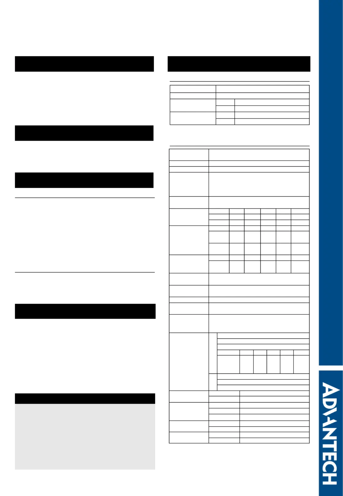
Packing ListSpecifications
User Manual
Declaration of Conformity
Overview
Notes
For more information on this and other Advantech
products, please visit our websites at:
http://www.advantech.com/eAutomation
For technical support and service:
http://www.advantech.com/support/
This startup manual is for PCI-1712/1712L.
Part No.20031712101st Edition
June 2007
Input Channels
16bi-directional
Number of Ports2
Input Voltage
Low0.8 V max.
High2.0V min.
Output Voltage
Low0.5 V max. @ + 24 mA (sink)
High2.4V min. @ - 15 mA (source)
Channels
16 single-ended or 8 differential or combi-
nation
Resolution12-bit
FIFO Size1K samples
Max. Sampling
Rate
Milti-channel, single gain: MS/s
Milti-channel, multi gain: 600kS/s
Milti-channel, multi gain, unipolar/bipolar:
400kS/s
Conversion
Time
500 ns
Input range
and Gain List
Gain0.51248
UnipolarN/A0~100~50~2.50~1.25
Bipolar±10±5±2.5±1.25±0.625
Drift
Gain0.51248
Zero(µV
/°C)
±80±30±30±30±30
Gain(pp
m/°C)
±30±30±30±30±30
Small Signal
Bandwidth for
PGA
Gain0.51248
Band-
width
4.0
MHz
4.0
MHz
2.0
MHz
1.5
MHz
0.65
MHz
Common Mode
Voltage
±11 V max. (operational)
Max. Input
Voltage
±20 V
Input Protect30 Vp-p
Input
Impedance
100 MΩ/10pF(Off); 100 MΩ/100pF(On)
Trigger Mode
Software, on-board programmable pacer
or external, pre-trigger, post-trigger, delay-
trigger, about-trigger
Accuracy
DC
DNLE: ±1LSB
INLE: ±3LSB
Offset error: < 1 LSB
Gain0.51248
Gain
error
(% FSR)
0.150.030.030.050.1
AC
SNR: 68 dB
ENOB: 11 bits
THD: -75 dB typical
External TTL
Trigger Input
Low0.8 V max.
High2.0 V min.
External Ana-
log Trigger
Input
Range-10V to + 10 V
Resolution8-bit
Impedence
100 MΩ/10 pF typical
Clock Output
Low0.5 V max.@ +24 mA
High2.4 V min. @ -15 mA
Trigger Output
Low0.5 V max.@ +24 mA
High2.4 V min. @ -15 mA
Product specificaties
| Merk: | Advantech |
| Categorie: | Niet gecategoriseerd |
| Model: | PCI-1712 |
Heb je hulp nodig?
Als je hulp nodig hebt met Advantech PCI-1712 stel dan hieronder een vraag en andere gebruikers zullen je antwoorden
Handleiding Niet gecategoriseerd Advantech

5 Juni 2026
5 Juni 2026
3 Juni 2026
2 Juni 2026
1 Juni 2026
1 Juni 2026
1 Juni 2026
27 Mei 2026
1 Mei 2026
29 April 2026
Handleiding Niet gecategoriseerd
Nieuwste handleidingen voor Niet gecategoriseerd
8 Juni 2026
8 Juni 2026
8 Juni 2026
8 Juni 2026
8 Juni 2026
8 Juni 2026
8 Juni 2026
8 Juni 2026
8 Juni 2026
8 Juni 2026