Texas Instruments LMK1D2106L Handleiding
Texas Instruments Niet gecategoriseerd LMK1D2106L
Bekijk gratis de handleiding van Texas Instruments LMK1D2106L (46 pagina’s), behorend tot de categorie Niet gecategoriseerd. Deze gids werd als nuttig beoordeeld door 2 mensen en kreeg gemiddeld 4.8 sterren uit 2 reviews. Heb je een vraag over Texas Instruments LMK1D2106L of wil je andere gebruikers van dit product iets vragen? Stel een vraag
Pagina 1/46
LMK1D210xL Ultra Low Additive Jitter LVDS Buffer
1 Features
•High-performance LVDS clock buffer family: up to
2GHz
–Dual 1:2 differential buffer
–Dual 1:4 differential buffer
–Dual 1:6 differential buffer
–Dual 1:8 differential buffer
•Supply voltage: 1.71V to 3.465V
•Dual output common mode voltage operation:
–Output common mode voltage: 0.7V at 1.8V
supply voltage.
–Output common mode voltage: 1.2V at 2.5V/
3.3V supply voltage
•Low additive jitter:
–< 17fs RMS typical in 12kHz to
20MHz at 1250.25MHz
–< 22fs RMS typical in 12kHz to
20MHz at 625MHz
–< 60fs RMS maximum in 12kHz to
20MHz at 156.25MHz
–Very low phase noise floor: -164dBc/Hz (typical
at 156.25MHz)
•Very low propagation delay: < 575ps maximum
•Output skew:
–15ps maximum (LMK1D2102, LMK1D2104)
–20ps maximum (LMK1D2106, LMK1D2106)
•Part to Part skew: 150ps
•High-swing LVDS (boosted mode): 500mV VOD
typical when AMP_SELA, AMP_SELB= Floating
•Bank enable/disable using AMP_SELA and
AMP_SELB Section 8.4.1
•Fail-safe input operation
•Universal inputs accept LVDS, LVPECL, LVCMOS,
HCSL and CML signal levels
•LVDS reference voltage, V
AC_REF
, available for
capacitive-coupled inputs
•Extended industrial temperature range: –40°C to
105°C
2 Applications
•Telecommunications and networking
•Medical imaging
•Test and measurement
•Wireless infrastructure
•Pro audio, video and signage
3 Description
The LMK1D210xL is a low noise dual clock buffer
which distributes one input to a maximum of 2
(LMK1D2102L), 4 (LMK1D2104L), 6 (LMK1D2106L)
or 8 (LMK1D2108L) LVDS outputs. The inputs can
either be LVDS, LVPECL, HCSL, CML, or LVCMOS.
The LMK1D210xL is specifically designed for driving
50Ω transmission lines. When driving inputs in single-
ended mode, apply the appropriate bias voltage to the
unused negative input pin (see Figure 8-8).
LMK1D210xL buffer offers two output common mode
operation (0.7V and 1.2V) for different operating
supply. The device provides flexibility in design for
DC-coupled mode applications.
AMP_SELA / AMP_SELB control pin can be used
to select different output amplitude LVDS (350mV)
or boosted LVDS (500mV). In addition to amplitude
selection, outputs can be disabled using the same pin.
The part also supports Fail-Safe Input function for
clock and digital input pins. The device further
incorporates an input hysteresis which prevents
random oscillation of the outputs in the absence of
an input signal.
Package Information
PART NUMBER
(1)
PACKAGEPACKAGE SIZE
(3)
LMK1D2102LRGT (VQFN, 16)3.00mm × 3.00mm
LMK1D2104LRHD (VQFN, 28)5.00mm × 5.00mm
LMK1D2106LRHA (VQFN, 40)6.00mm × 6.00mm
LMK1D2108L
(2)
RGZ (VQFN, 48)7.00mm × 7.00mm
(1)For all available packages, see the orderable addendum at
the end of the data sheet.
(2)Preview only.
(3)The package size (length × width) is a nominal value and
includes pins, where applicable.
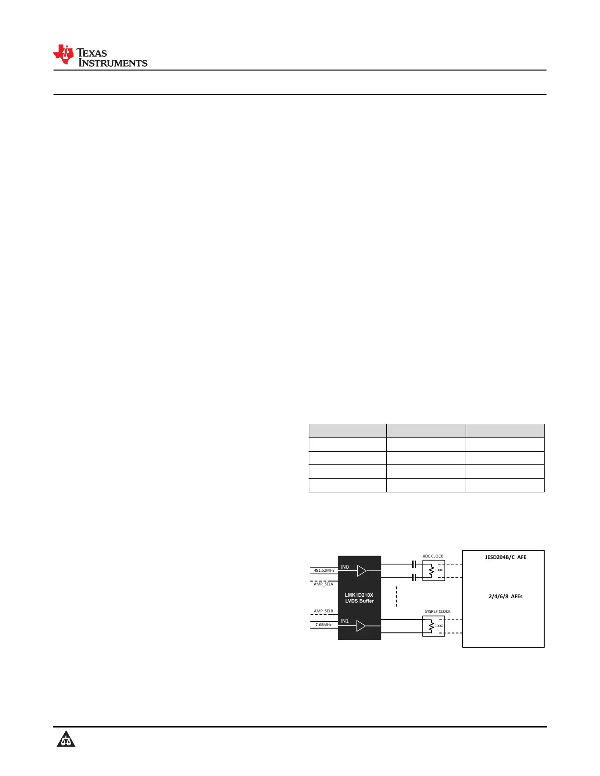
100Ω
ADCCLOCK
100Ω
SYSREFCLOCK
491.52MHz
7.68MHz
JESD204B/CAFE
2/4/6/8AFEs
LMK1D210X
LVDSBuffer
IN0
IN1
AMP_SELA
AMP_SELB
Application Example
LMK1D2102L, LMK1D2104L, LMK1D2106L, LMK1D2108L
SNAS888A – SEPTEMBER 2024 – REVISED NOVEMBER 2024
An IMPORTANT NOTICE at the end of this data sheet addresses availability, warranty, changes, use in safety-critical applications,
intellectual property matters and other important disclaimers. PRODUCTION DATA.
Product specificaties
| Merk: | Texas Instruments |
| Categorie: | Niet gecategoriseerd |
| Model: | LMK1D2106L |
Heb je hulp nodig?
Als je hulp nodig hebt met Texas Instruments LMK1D2106L stel dan hieronder een vraag en andere gebruikers zullen je antwoorden
Handleiding Niet gecategoriseerd Texas Instruments

23 Juli 2026
23 Juli 2026
22 Juli 2026
21 Juli 2026
21 Juli 2026
21 Juli 2026
21 Juli 2026
20 Juli 2026
20 Juli 2026
20 Juli 2026
Handleiding Niet gecategoriseerd
Nieuwste handleidingen voor Niet gecategoriseerd
23 Juli 2026
23 Juli 2026
23 Juli 2026
23 Juli 2026
23 Juli 2026
23 Juli 2026
23 Juli 2026
22 Juli 2026
22 Juli 2026
22 Juli 2026