Texas Instruments ADC3908D025 Handleiding
Texas Instruments Niet gecategoriseerd ADC3908D025
Bekijk gratis de handleiding van Texas Instruments ADC3908D025 (47 pagina’s), behorend tot de categorie Niet gecategoriseerd. Deze gids werd als nuttig beoordeeld door 10 mensen en kreeg gemiddeld 5.0 sterren uit 6 reviews. Heb je een vraag over Texas Instruments ADC3908D025 of wil je andere gebruikers van dit product iets vragen? Stel een vraag
Pagina 1/47
ADC3908Dx and ADC3908Sx 8-bit, 25 to 125MSPS Low Latency, Low Power, Small,
Single and Dual Channel ADC with Integrated Input Buffers
1 Features
•Sampling rate up to 125MSPS
•Latency: 1 clock cycle
•Low power (2 channel):
–90mW at 125MSPS
–56mW at 25MSPS
–3mW in PD mode
•Small footprint: 32-VQFN (4mm x 4mm)
•Single or dual channel ADC
•Internal reference
•No missing codes, ±0.25 LSB INL
•Buffered, differential or single ended inputs
•Input bandwidth: 150MHz (3dB)
•Single 1.8V supply
–Optional 3.3V
IO
capability
•Industrial temperature range: -40°C to 105°C
•Parallel (SDR, DDR) CMOS interface
•Spectral performance (FS
CLK
= 125MSPS, f
IN
= 5
MHz):
–SNR: 49.8dBFS
–SFDR: 60dBFS
2 Applications
•Low latency control loops
•Laser scanners
•Displacement sensors
•Detection equipment
3 Description
The ADC3908Dx and ADC3908Sx are a family
of ultra-low power 8-bit 125MSPS high-speed dual
and single channel analog-to-digital converters. High-
speed control loops benefit from the short latency of
only 1 clock cycle. The ADC consumes only 90mW at
125MSPS with a power consumption that scales with
lower sampling rates.
The ADC3908Dx and ADC3908Sx uses parallel DDR
or SDR CMOS interface to output the data, and can
be driven at +1.8V or +3.3V to accommodate various
receiver requirements. The analog input and output
interface can be easily configured via pin control
(Interface Configuration Table). The device is a pin-
to-pin compatible family of ADCs with 8 and 10-bit
resolution and different speed grades. The device is
available in a 32-pin VQFN package, and supports
industrial temperature range from -40 to +105°C.
Package Information
PART NUMBERPACKAGE
(1)
PACKAGE SIZE
(2)
ADC3908D025,
'D065, 'D125
ADC3908S025,'S06
5, 'S125
VQFN (32)4mm × 4mm
(1)For more information, see Section 11.
(2)The package size (length × width) is a nominal value and
includes pins, where applicable.
Device Information
PART NUMBER
(c= #CH; sss= MSPS)
RESOLUTION
SAMPLING RATE
MSPS
ADC3910csss10-Bit25, 65, 125
ADC3908csss8-Bit25, 65, 125
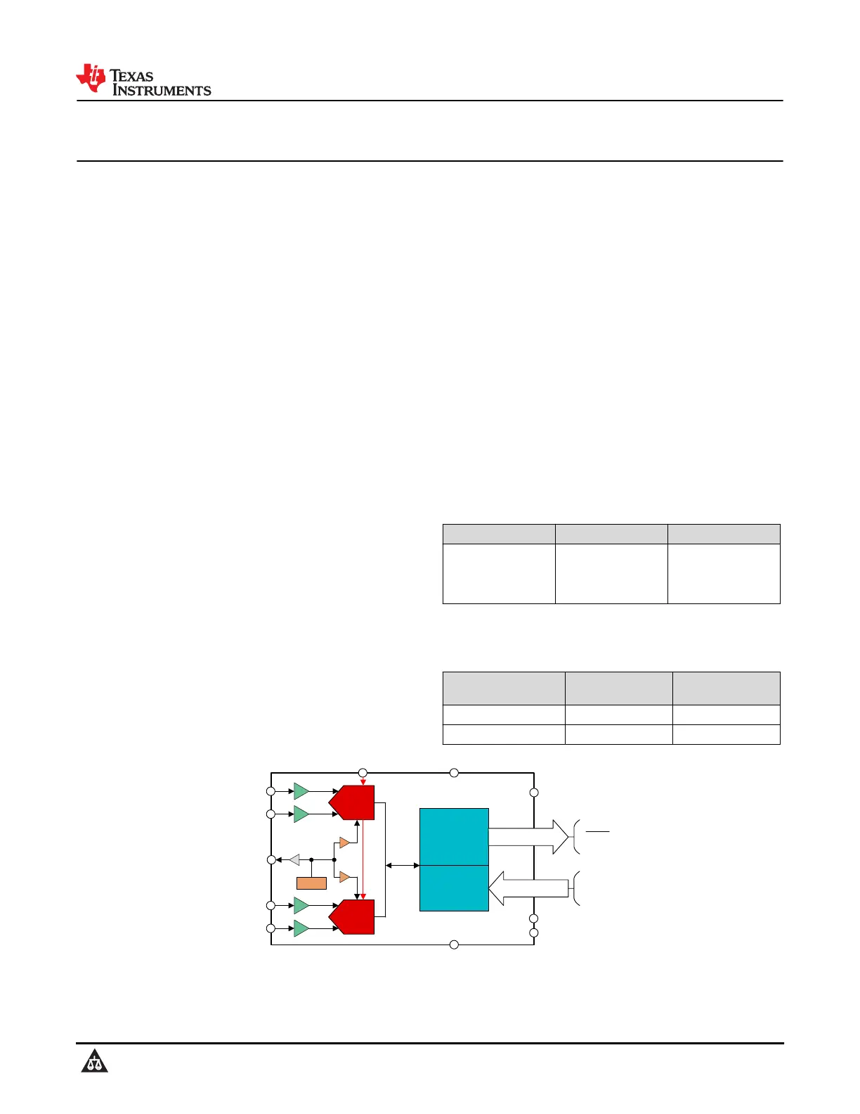
REF
ADC
ADC
Parallel
Interface
Control
Interface
RESET
AVDD
IOVDD
CLK
GND
M2
M1
M0
INAP
INAM
INBP
INBM
VCM
DCLK
DCLK
#8 DOUT
PDN
Block Diagram
ADC3908D025, ADC3908D065, ADC3908D125
ADC3908S025, ADC3908S065, ADC3908S125
SBASAU9 – OCTOBER 2024
An IMPORTANT NOTICE at the end of this data sheet addresses availability, warranty, changes, use in safety-critical applications,
intellectual property matters and other important disclaimers. PRODUCTION DATA.
Product specificaties
| Merk: | Texas Instruments |
| Categorie: | Niet gecategoriseerd |
| Model: | ADC3908D025 |
Heb je hulp nodig?
Als je hulp nodig hebt met Texas Instruments ADC3908D025 stel dan hieronder een vraag en andere gebruikers zullen je antwoorden
Handleiding Niet gecategoriseerd Texas Instruments

23 Juli 2026
23 Juli 2026
22 Juli 2026
21 Juli 2026
21 Juli 2026
21 Juli 2026
21 Juli 2026
20 Juli 2026
20 Juli 2026
20 Juli 2026
Handleiding Niet gecategoriseerd
Nieuwste handleidingen voor Niet gecategoriseerd
23 Juli 2026
23 Juli 2026
23 Juli 2026
23 Juli 2026
23 Juli 2026
23 Juli 2026
23 Juli 2026
22 Juli 2026
22 Juli 2026
22 Juli 2026